Step 1
| 1 | Open a new project with File > New > Single Fiber. |
| 2 | Calculation > Inverse Scattering Solver, to get Inverse Problem Solver dialog box. |
| 3 | Select User Defined frame checkbox. |
| 4 | Enter the starting and ending wavelengths, and the number of steps in the User-Defined frame as shown. |

- The Steps field indicates the number of divisions used in the specified wavelength
range.
| 5 | In the Length field, enter the length of the grating, 5 cm (50,000 μm). |
| 6 | In the Segments field, enter the number of segments to be 1000, this is the number of segments that will have constant coupling coefficients within them. The layer peeling algorithm will use 1000 layers in this case. |
| 7 | Enter 4 in the Over Sample field. Over Sample is used in the reconstruction of the truncated impulse response, the accuracy is sometimes improved by using finer steps in the spectrum. |
| 8 | Click on the Define button next to the Ref/Trans. |
This brings up a dialog box for defining the reflectivity spectrum as seen below:
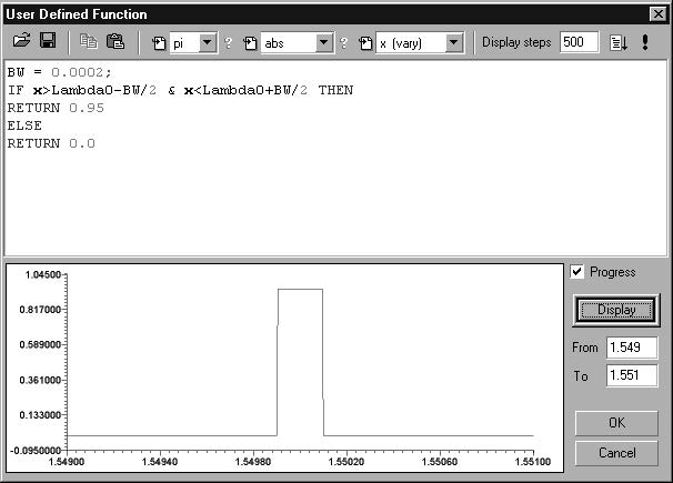
| 9 | Next, type in the text as shown in the screen above. |
| 10 | Click on Display to plot the curve shown. The desired impulse response will be calculated from the Fourier transform of this reflection coefficient. |
| 11 | Click OK. |
| 12 | Click on the Disp button in the Inverse Problem Solver dialog box. This means that we will define the phase response by specifying dispersion. |
| 13 | Click on the adjacent Define button to define the dispersion profile. This will produce the following results: |
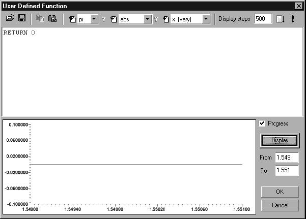
- Here the dispersion returned is 0 for all wavelengths in the range.
| 14 | Click OK |
Step 2
| 1 | Click on the Causality button in the Inverse Problem Solver dialog box. This will display the impulse response calculated from the spectrum you have defined. |
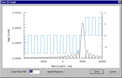
- Because of causality, any real impulse response must be zero for negative
arguments. In this picture some unphysical oscillations are seen in the negative
domain. These oscillations will cause inaccuracies in the reconstruction. They
can be reduced by adding delay to the response (a linear phase shift).
Note: You can experiment with various delays by entering other numbers in the
Linear Phase Shift field, and clicking Impulse Response to see the result.
| 2 | Click on Close. |
| 3 | Click on Start in the Inverse Problem Solver dialog box to start the reconstruction. A progress bar indicates the progress of the layer peeling algorithm. When this process finishes, the reconstructed grating profile is used to generate the spectrum of the new grating. A second progress bar displays the progress of the calculation of the spectrum. |
| 4 | Select the Power tab to see the spectrum of the new grating |
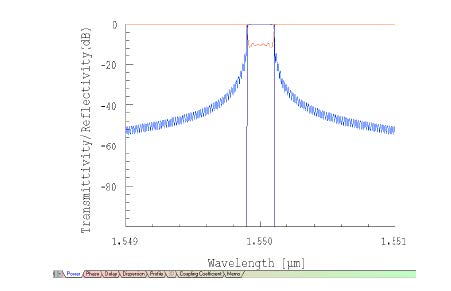
| 5 | The realised Reflectivity is shown in light blue, and the desired reflectivity in dark blue. The Transmission is shown in red. |
| 6 | Select the Dispersion Tab to show the realized versus the desired dispersion. |
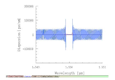
- Within the reflection band, where significant power is reflected, the dispersion is
close to the desired value. The dispersion outside the reflection band comes from
the very small reflection in this spectral range, and the desired response is lost in
numerical noise.
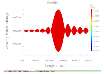
| 7 | Select the Profile tab to see the actual grating which generated this spectrum. |