Optiwave software can be used in different industries and applications, including Fiber Optic Communication, Sensing, Pharma/Bio, Military & Satcom, Test & Measurement, Fundamental Research, Solar Panels, Components / Devices, etc..
OptiSystem is a comprehensive software design suite that enables users to plan, test, and simulate optical links in the transmission layer of modern optical networks.
OptiSPICE is the first circuit design software for analysis of integrated circuits including interactions of optical and electronic components. It allows for the design and simulation of opto-electronic circuits at the transistor level, from laser drivers to transimpedance amplifiers, optical interconnects and electronic equalizers.
OptiFDTD is a powerful, highly integrated, and user friendly CAD environment that enables the design and simulation of advanced passive and non-linear photonic components.
OptiBPM is a comprehensive CAD environment used for the design of complex optical waveguides. Perform guiding, coupling, switching, splitting, multiplexing, and demultiplexing of optical signals in photonic devices.
OptiFiber The optimal design of a given optical communication system depends directly on the choice of fiber parameters. OptiFiber uses numerical mode solvers and other models specialized to fibers for calculating dispersion, losses, birefringence, and PMD.
Emerging as a de facto standard over the last decade, OptiGrating has delivered powerful and user friendly design software for modeling integrated and fiber optic devices that incorporate optical gratings.
OptiConverge is a collaborative integration framework that seamlessly combines two or more Optiwave products (e.g., OptiSystem, OptiSPICE, OptiFDTD, etc.) and other third party products into unified solutions. Designed to streamline complex workflows, it empowers users to achieve their goals faster by harnessing the collective power of our trusted Optiwave tools.
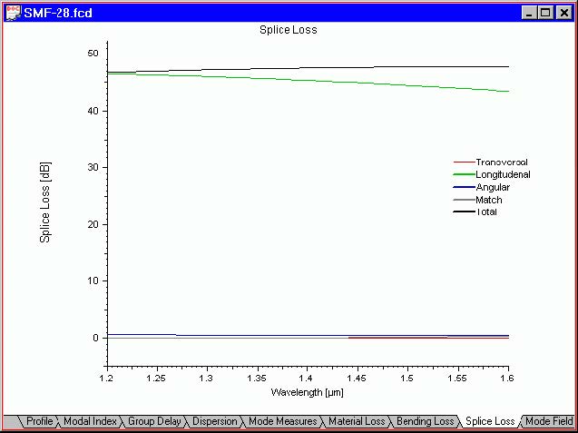
The “Splice Loss” view shows you the transversal, longitudinal, and angular
misalignment loss, as well as the mode match and total splice loss vs. the scan
parameter. The default scan parameter is the wavelength. You can change the scan
parameter in the “Properties of Fundamental Mode” dialog box.
To access this view do one of the following steps:
Step
Action
1
Select the “Splice Loss” tab in the “Views” window
2
Select “Views/Splice Loss” on the “View” menu
Mode Field view
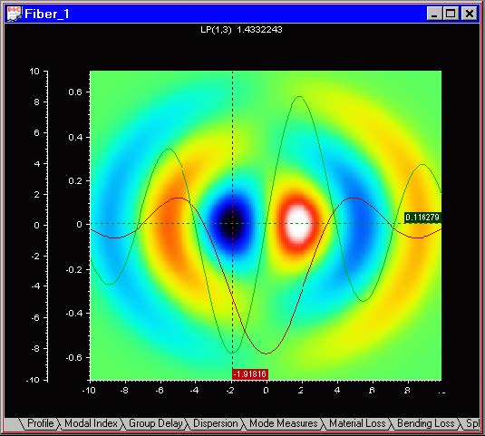
The “Mode Field” view shows you a topographic plot of the mode field. The displayed
mode is the one selected in the Modes dialog box. You can change the display mesh
in the Global Settings dialog box. Also a X- or Y-cuts (or both) of the mode are shown.
To access this view do one of the following steps:
Step
Action
1
Select the “Mode Field” tab in the “Views” window
2
Select “Views/Mode Field” on the “View” menu
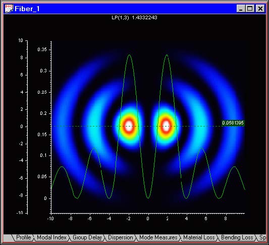
If the option “Amplitude”, instead of “Intensity” has been selected from the right-button
context menu “Graph Properties”, then the ”Mode Field” displays a topological color coded pattern and 2D X- and Y-cut cross sections of the amplitude of the same field, as shown below: