Most of the photonic crystal has the periodic lattice. In some cases, you may want to know the band gap effect for such a lattice. As discussed in the OptiFDTD Technical Background, this task can be simplified in an FDTD simulation using plane wave excitation and PEC/PMC boundary conditions.
For example, Figure 100 shows a 2D square lattice going to infinity in both x- and z directions.
Figure 100: 2D square lattice
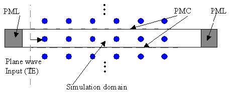
You can simulate the structure shown in Figure 100 by taking a domain-reduced
region (shown in Figure 101) with a plane wave and PMC boundary conditions for 2DTE
wave.
Figure 101: Domain reduced region
Designing a PBG structure
To design a PBG structure, perform the following procedures.
| Step | Action |
| 1 | Start Waveguide Layout Designer. |
| 2 | To create a new project, select File > New.
The Initial Properties dialog box appears. |
| 3 | Click Profiles and Materials.
The Profile Designer window appears. |
| 4 | Under the Materials folder of OptiFDTD Designer1, right-click the Dielectric folder and select New.
A new Dielectric material dialog box appears. |
| 5 | Type the following information:
Name: PBG_atom Refractive index (Re:): 3.1 |
| 6 | To save the material, click Store.
PBG_atom appears in the Dielectric folder in the directory and in the dialog box title bar. |
To define the channel profile, perform the following procedure.
| Step | Action |
| 1 | Under the Profiles folder of OptiFDTD Designer1, right-click the Channel folder and select New.
The ChannelPro1 dialog box appears. |
| 2 | Create the following channel profile:
Profile name: Profile_PBG 2D profile definition Material: PBG_atom 3D profile definition Layer name: layer_01 Width: 1.0 Thickness: 1.0 Offset: 0.0 Material: PBG_atom |
| 3 | Click Store. |
| 4 | Close the Profile Designer. |
To define the wafer and waveguide properties, perform the following procedure.
| Step | Action |
| 1 | In the Initial Properties dialog box, type/select the following:
Waveguide Properties Width [μm]: 1.0 Profile: Profile_PBG Wafer Dimensions Length [μm]: 10.0 Width [μm]: 1.0 2D Wafer Properties Material: Air |
| 2 | Click OK.
The Initial Properties dialog box closes. |
| 3 | In the Layout Designer, from the Draw menu, select PBG Crystal Structure. |
| 4 | In the layout window, drag the cursor from a designated starting point and release, to create the PBG area.
The PBG Crystal Structure appears in the layout window. |
| 5 | To edit the crystal structure, double-click on the PBG structure in the layout.
The Crystal Lattice Properties dialog box appears (see Figure 86 as a reference). |
| 6 | In Origin, Offset, type/select the following:
Horizontal: 2.0 Vertical: -0.5 |
| 7 | Click Evaluate. |
| 8 | Type/select the following:
Depth: 0.0 Azimuth [deg]: 0.0 |
| 9 | In Lattice Properties, select 2D Rectangular. |
| 10 | In Lattice Dimensions, type/select the following:
Scale: 1.0 #A: 1 #C: 6 Note: When a 2D lattice is selected, the Y-direction cell #B is set to the default value of 1. |
| 11 | In Label, type PBGCrystalStruct1.
Note: Do NOT close the Crystal Lattice Properties dialog box. |
Setting the atom properties
To set the atom properties, perform the following procedure in the Crystal Lattice Properties dialog box.
| Step | Action |
| 1 | In Atom Waveguide in Unit Cell, Add New, select Elliptic Waveguide from the drop-down menu and click New.
The Elliptic Waveguide Properties dialog box appears (see Figure 87 as a reference). |
| 2 | In Center, Offset, type/select the following:
Horizontal: 0.5 Vertical: 0.5 |
| 3 | Type/select the following:
Major radius: 0.2 Minor radius: 0.2 Orientation angle: 0.0 Channel thickness tapering: Use Default (Channel: None) Depth: 0.0 Label: Atom Profile: Profile_PBG. |
| 4 | Click OK to close the Elliptic Waveguide Properties dialog box.
Note: When you return to the Crystal Lattice Properties dialog box, you will see the defined elliptic waveguide listed in Atom Waveguide in Unit Cell. |
| 5 | Click OK to close the Crystal Lattice Properties dialog box.
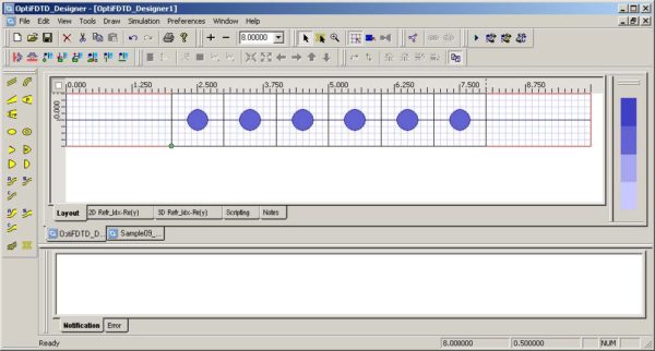
The defined PBG structure appears in the layout window (see Figure 102). |
Figure 102: Defined PBG structure in layout window
Inserting the input plane
To insert the input plane, perform the following procedure.
| Step | Action |
| 1 | From the Draw menu, select Vertical Input Plane. |
| 2 | To insert the input plane, click in the layout window where you want it placed.
The input plane appears in the layout. |
| 3 | To edit the input plane, double-click on the input plane in the layout.
The Input Plane Properties dialog box appears. |
| 4 | Set Wavelength to 1.9 mm |
| 5 | Select Gaussian Modulated Continuous Wave. |
| 6 | On the Gaussian Modulated CW tab, type/select the following: Time Offset [Sec]: 6.0e-14
Half Width [Sec]: 1.0e-14 |
| 7 | On the General tab, select Input Field Transverse: Rectangular. |
| 8 | On the 2D Transverse tab, type/select the following:
Center Position [μm]: 0.0 Halfwidth [μm]: 2.0 Tilting Angle [deg]: 0.0 Effective Refractive Index: Local Amplitude [V/m]: 1.0 |
| 9 | On the General tab, type/select the following:
Plane Geometry Z Position [μm]: 0.5 Positive direction |
| 10 | Click OK.
The Input Field Properties dialog box closes. |
Setting up the Observation Point
| Step | Action |
| 1 | From the Draw menu, select Observation Point. |
| 2 | Place the Observation Point in the desired position in the layout. |
| 3 | Double-click the observation point.
The Observation Properties — Point dialog box appears. |
| 4 | On the General tab:
In Center, Offset, type/select the following: Horizontal: 0.25μm Vertical: 0.0μm Center depth: 0.0 μm Label: Observation Point1 |
| 5 | On the Data Components tab, ensure that 2D TE: Ey is selected (default). |
| 6 | Click OK.
The Observation Properties — Point dialog box closes. |
| 7 | Repeat steps 1 to 5 and create another Observation Point with the following information. |
| 8 | On the General tab:
In Center, Offset, type/select the following: Horizontal: 8.5μm Vertical: 0.0μm Center depth: 0.0 μm Label: Observation Point2 |
| 9 | On the Data Components tab, ensure that 2D TE: Ey is selected (default). |
| 10 | Repeat steps 1 to 5 and create another Observation Point with the following information. |
| 11 | On the General tab:
In Center, Offset, type/select the following: Horizontal: 9.5μm Vertical: 0.0μm Center depth: 0.0 μm Label: Observation Point3 |
| 12 | On the Data Components tab, ensure that 2D TE: Ey is selected (default).
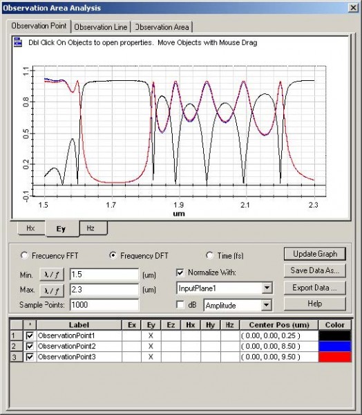
Note: Observation Point1 is used to calculate the reflection, while Observation Point2 and Observation Point3 are used to calculate the transmittance. |
Setting the 2D TE FDTD simulation parameters
| Step | Action |
| 1 | From the Simulation menu, select 2D Simulation Parameters.
The Simulation Parameters dialog box appears. |
| 2 | Type/select the following information:
Polarization: TE Mesh Delta X [μm]: 0.05 Mesh Delta Y [μm]: 0.05 |
| 3 | Click Advanced….
The Boundary Conditions dialog box appears. |
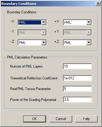
| 4 | Type/select the following information (see Figure 103):
-X: Anisotropic PML +X: Anisotropic PML -Z: Anisotropic PML +Z: Anisotropic PML Anisotropic PML Calculation Parameters Number of Anisotropic PML Layers: 10 Theoretical Reflection Coefficient: 1.0e-12 Real Anisotropic PML Tensor Parameters: 5.0 Power of Grading Polynomial: 3.5 Figure 103: 2D simulation parameters Note: The rectangular beam with PMC boundaries on the edge realizes the TE plane wave simulation for the periodic structure. |
| 5 | In Time Parameters, click Calculate. The default time step size is calculated. |
| 6 | Select Run for 12000 Time Steps (Results Finalized). |
| 7 | Select Key Input Information: Input Plane1 and wavelength:1.9.Note: The input plane’s center wavelength is used for DFT calculations. |
| 8 | Click OK to close the Simulation Parameters dialog box without running the simulation, or click Run to start the OptiFDTD Simulator.Note: Before running the simulation, save the project to a file. |
Observing the simulation results in OptiFDTD Simulator
Key things to observe:
- Refractive index distribution
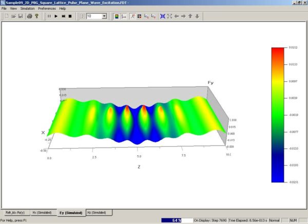
- Observe the wave propagation in OptiFDTD Simulator (see Figure 104).
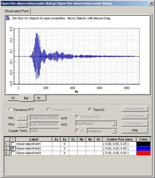
- Select View > Observation Point to see the dynamic time domain and frequency domain response (see Figure 105).
Figure 104: OptiFDTD Simulator—Wave propagation
Figure 105: OptiFDTD Simulator—Dynamic time domain and frequency domain response
Performing data analysis
In OptiFDTD_Analyzer, perform the following procedure.
| Step | Action |
| 1 | To start the observation point analysis, from the Tools menu, select Observation Area Analysis.
The Observation Area Analysis dialog box appears (see Figure 99). |
| 2 | Select ObservationPoint1, ObservationPoint2, and ObservationPoint3.
The simulation results from the observation points displays in the graph window. |
| 3 | Type/select the following:
Frequency DFT Min. λ /f : 1.5μm Max. λ /f : 2.3μm Sample Point: 1000 Normalize With InputPlane1 |
| 4 | Click Update Graph to view the transmittance and reflection curves (see Figure 106). |
Figure 106: Observation Area Analysis dialog box


