Optiwave software can be used in different industries and applications, including Fiber Optic Communication, Sensing, Pharma/Bio, Military & Satcom, Test & Measurement, Fundamental Research, Solar Panels, Components / Devices, etc..
OptiSystem is a comprehensive software design suite that enables users to plan, test, and simulate optical links in the transmission layer of modern optical networks.
OptiSPICE is the first circuit design software for analysis of integrated circuits including interactions of optical and electronic components. It allows for the design and simulation of opto-electronic circuits at the transistor level, from laser drivers to transimpedance amplifiers, optical interconnects and electronic equalizers.
OptiFDTD is a powerful, highly integrated, and user friendly CAD environment that enables the design and simulation of advanced passive and non-linear photonic components.
OptiBPM is a comprehensive CAD environment used for the design of complex optical waveguides. Perform guiding, coupling, switching, splitting, multiplexing, and demultiplexing of optical signals in photonic devices.
OptiFiber The optimal design of a given optical communication system depends directly on the choice of fiber parameters. OptiFiber uses numerical mode solvers and other models specialized to fibers for calculating dispersion, losses, birefringence, and PMD.
Emerging as a de facto standard over the last decade, OptiGrating has delivered powerful and user friendly design software for modeling integrated and fiber optic devices that incorporate optical gratings.
OptiConverge is a collaborative integration framework that seamlessly combines two or more Optiwave products (e.g., OptiSystem, OptiSPICE, OptiFDTD, etc.) and other third party products into unified solutions. Designed to streamline complex workflows, it empowers users to achieve their goals faster by harnessing the collective power of our trusted Optiwave tools.
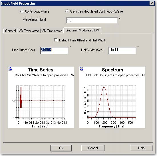
• Right click on the time domain and spectrum domain graph. Select the Zoom tool and highlight the required area to enlarge it. This way you can read the bandwidth. Double click the graph to return to the original view.
Note:
• The following is time domain formula for Gaussian Modulated Continuous Wave. Its corresponding spectrum also has Gaussian shape.
Where t0 is the time offset and T is the half width and
wavelength λ0 is the center.
• Time Offset is the time difference between the time zero and Gaussian envelop peak value position. Time offset should keep the time domain beam in a full Gaussian envelop, i.e. time domain start value should be close to zero at time zero and convergent to zero after a short time distance far before the total simulated time.
• Time domain half width controls the Gaussian envelop size. If this value is smaller, then the corresponding spectrum will become larger.
• We can always adjust Time Offset and Half Width to realize a certain bandwidth.
• This time domain formula cannot hold effective Bandwidth (bandwidth/center wavelength) larger than 75%. In case of a super broad band simulation, the simulation must be split into several bandwidth.
• The default value will be at least 60% of the effective bandwidth.
5
Set transverse beam pattern:
• Set Modal as Input Field Transverse under General tab
• Z Position (µm) : 1.0
• Positive direction.
• Initial phase (deg): 0.0
• Click 2D transverse tab to solve the mode. Apply the solve mode as input field. If you are not familiar with this step, please refer to tutorial lesson 2 as a reference.