Optiwave software can be used in different industries and applications, including Fiber Optic Communication, Sensing, Pharma/Bio, Military & Satcom, Test & Measurement, Fundamental Research, Solar Panels, Components / Devices, etc..
OptiSystem is a comprehensive software design suite that enables users to plan, test, and simulate optical links in the transmission layer of modern optical networks.
OptiSPICE is the first circuit design software for analysis of integrated circuits including interactions of optical and electronic components. It allows for the design and simulation of opto-electronic circuits at the transistor level, from laser drivers to transimpedance amplifiers, optical interconnects and electronic equalizers.
OptiFDTD is a powerful, highly integrated, and user friendly CAD environment that enables the design and simulation of advanced passive and non-linear photonic components.
OptiBPM is a comprehensive CAD environment used for the design of complex optical waveguides. Perform guiding, coupling, switching, splitting, multiplexing, and demultiplexing of optical signals in photonic devices.
OptiFiber The optimal design of a given optical communication system depends directly on the choice of fiber parameters. OptiFiber uses numerical mode solvers and other models specialized to fibers for calculating dispersion, losses, birefringence, and PMD.
Emerging as a de facto standard over the last decade, OptiGrating has delivered powerful and user friendly design software for modeling integrated and fiber optic devices that incorporate optical gratings.
OptiConverge is a collaborative integration framework that seamlessly combines two or more Optiwave products (e.g., OptiSystem, OptiSPICE, OptiFDTD, etc.) and other third party products into unified solutions. Designed to streamline complex workflows, it empowers users to achieve their goals faster by harnessing the collective power of our trusted Optiwave tools.
To add a new profile to the Profile Designer, perform the following procedure.
Step
Action
1
Double-click on the waveguide in the layout window.
The Linear Waveguide Properties dialog box appears.
2
Click Profiles in Use.
The Profile Designer opens.
3
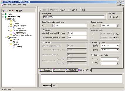
Right-click on Diffusion profile Mg:LiNbO3 and create a new profile: Name: Mg:LiNbO3_1
Stripe thickness before diffusion: 0.004
Diffusion length in depth: 2
Lateral diffusion length: 4.0
4
Return to the layout window.
Creating the top linear waveguide
To draw a new linear waveguide of the same width (6 μm) on top of the Ti diffused one, perform the following procedure.
Step
Action
1
Copy (Ctrl-C) and paste (Ctrl-V) the original waveguide in the layout
window.
A second linear waveguide appears in the layout window on top of the original one.
2
Double-click on the new waveguide to open the waveguide properties dialog box.
3
Change the Profile in Use to Mg:LiNbO3_1 (see Figure 11).
Figure 10: Linear Waveguide Properties dialog box—new waveguide
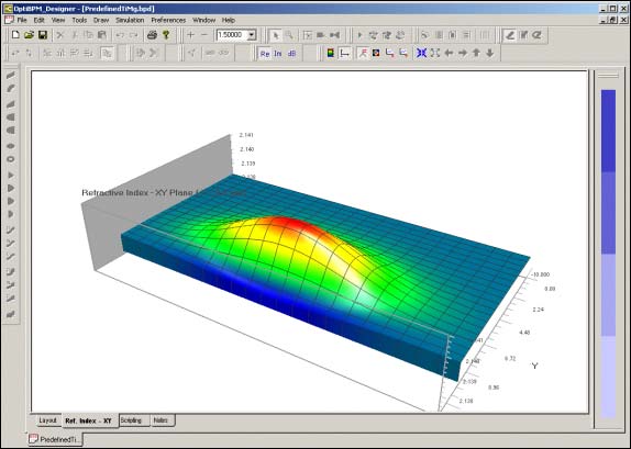
Note: Since the diffused processes are additive, the top waveguide is not going to overwrite the bottom waveguide but both processes will contribute to the final refractive index distribution. You can check the index distribution in the designer by going to the Ref.Index tab (see Figure 12).
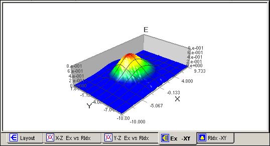
You can now run the 3D simulation (see Figure 13 and Figure 14 for 3D results).
Figure 11: Mg:LiNb03_1 profile
Figure 12: Refractive Index 3D view
In diffused waveguides, the refractive index is small. To view the diffusion, set the scale manually:
Step
Action
1
Right-click on the graph.
2
Select Data Clamping Settings.
3
Unselect the Auto scale.
4
Enter Min = 2.137 and Max = 2.142
5
Click Apply.
Note: Auto scale will stay off until you turn it back on, so don’t forget to turn Auto scale back on when viewing other data.