Optiwave software can be used in different industries and applications, including Fiber Optic Communication, Sensing, Pharma/Bio, Military & Satcom, Test & Measurement, Fundamental Research, Solar Panels, Components / Devices, etc..
OptiSystem is a comprehensive software design suite that enables users to plan, test, and simulate optical links in the transmission layer of modern optical networks.
OptiSPICE is the first circuit design software for analysis of integrated circuits including interactions of optical and electronic components. It allows for the design and simulation of opto-electronic circuits at the transistor level, from laser drivers to transimpedance amplifiers, optical interconnects and electronic equalizers.
OptiFDTD is a powerful, highly integrated, and user friendly CAD environment that enables the design and simulation of advanced passive and non-linear photonic components.
OptiBPM is a comprehensive CAD environment used for the design of complex optical waveguides. Perform guiding, coupling, switching, splitting, multiplexing, and demultiplexing of optical signals in photonic devices.
OptiFiber The optimal design of a given optical communication system depends directly on the choice of fiber parameters. OptiFiber uses numerical mode solvers and other models specialized to fibers for calculating dispersion, losses, birefringence, and PMD.
Emerging as a de facto standard over the last decade, OptiGrating has delivered powerful and user friendly design software for modeling integrated and fiber optic devices that incorporate optical gratings.
OptiConverge is a collaborative integration framework that seamlessly combines two or more Optiwave products (e.g., OptiSystem, OptiSPICE, OptiFDTD, etc.) and other third party products into unified solutions. Designed to streamline complex workflows, it empowers users to achieve their goals faster by harnessing the collective power of our trusted Optiwave tools.
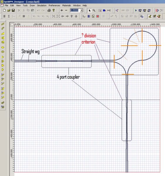
In the same manner, we may analyze the second design. There is no difference between this layout and the first. The simulation time savings are even more evident. Note the empty space occupying the bottom left section of the layout shown in Figure 15.
We follow exactly the same procedure as shown before. At this point, we want to point out the possible questionableness of any chosen division criteria. The optical sub- cells like the couplers should cover the entire functionality of the element. The slight difficulty arises with the division of the long curved waveguides marked on the Figure 15 with yellow lines. A user will probably pick the proposed solution marked by the bold lines. However, a potential success of the simulation will depend on the numerical method and/or approach employed for the particular task (e.g. the conformal mapping technique in cases of bent waveguides). This is shown by the thinner lines. Actually, a user is quite free when analyzing such the structure. We see it as an extra flexibility and our already gained experience shows, it really helps to understand the device behavior in every tiny detail.
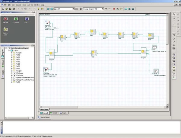
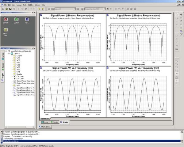
The MZI under the OptiSystem layout is shown on the next schematics (Figure 16 ). The explanation is simple. We have the input and the output couplers and two arms, the lower is characterized by one single bent waveguide, however the upper arm consist of the proper set of curved waveguides (any details are given in the manuals accordingly). The last graphics shows nothing else, but the interference patterns in the both output arms having the well-know shapes.
Figure 16: Mach-Zehnder system schematic in OptiSystem