Optiwave software can be used in different industries and applications, including Fiber Optic Communication, Sensing, Pharma/Bio, Military & Satcom, Test & Measurement, Fundamental Research, Solar Panels, Components / Devices, etc..
OptiSystem is a comprehensive software design suite that enables users to plan, test, and simulate optical links in the transmission layer of modern optical networks.
OptiSPICE is the first circuit design software for analysis of integrated circuits including interactions of optical and electronic components. It allows for the design and simulation of opto-electronic circuits at the transistor level, from laser drivers to transimpedance amplifiers, optical interconnects and electronic equalizers.
OptiFDTD is a powerful, highly integrated, and user friendly CAD environment that enables the design and simulation of advanced passive and non-linear photonic components.
OptiBPM is a comprehensive CAD environment used for the design of complex optical waveguides. Perform guiding, coupling, switching, splitting, multiplexing, and demultiplexing of optical signals in photonic devices.
OptiFiber The optimal design of a given optical communication system depends directly on the choice of fiber parameters. OptiFiber uses numerical mode solvers and other models specialized to fibers for calculating dispersion, losses, birefringence, and PMD.
Emerging as a de facto standard over the last decade, OptiGrating has delivered powerful and user friendly design software for modeling integrated and fiber optic devices that incorporate optical gratings.
OptiConverge is a collaborative integration framework that seamlessly combines two or more Optiwave products (e.g., OptiSystem, OptiSPICE, OptiFDTD, etc.) and other third party products into unified solutions. Designed to streamline complex workflows, it empowers users to achieve their goals faster by harnessing the collective power of our trusted Optiwave tools.
Hello Miguel, I have gone through all the parameters of the attached file and I found out that in profiles and materials the 2D profile defination should be same as that of 3D. Even the material should be same in wafer properties. You can just check it out.
Hi Harikiranjeet, as far the difference is concerned they are different in geometrical shape and also with respect to irreduicable Brillouin zone along the k vector path. Simulation is you have to choose what type of crystal you want and accordingly create the defect to create any sort of waveguide. Well I would say the hexagonal arrangement is much better for propagation of modes and output power is significantly better and thus the loss is.
Thanks again. But hey Ravil have you got any book with you named -“Photonic Crystals, Theory, Applications and Fabrication by Dennis W PratherC”. If so can you just attach the pdf file.
Under the FDTD-Nonlinear folder right click and create a new Material. From there you can choose whether it is a 2nd, 3rd, Kerr … type material. Since you only have the nonlinear index that means to me that you would be making a 3rd order material. You then just need to convert the index to a susceptibility. You can find the calculation on the web.
Hi Aurelien,
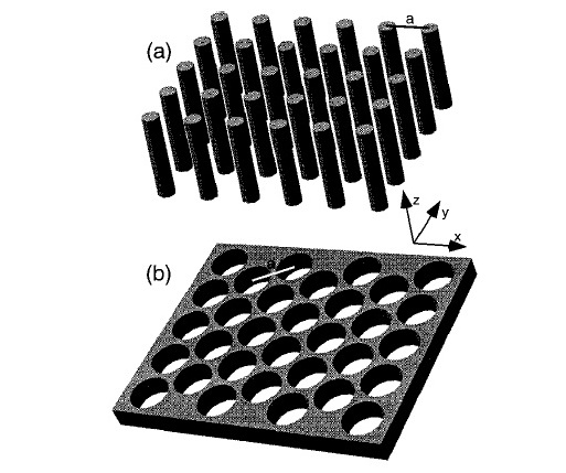
Yes you can check the paper “PHYSICAL REVIEW B VOLUME 60, NUMBER 8 15 AUGUST 1999”. Here I am attaching an image file, you can check it out.