Optiwave software can be used in different industries and applications, including Fiber Optic Communication, Sensing, Pharma/Bio, Military & Satcom, Test & Measurement, Fundamental Research, Solar Panels, Components / Devices, etc..
OptiSystem is a comprehensive software design suite that enables users to plan, test, and simulate optical links in the transmission layer of modern optical networks.
OptiSPICE is the first circuit design software for analysis of integrated circuits including interactions of optical and electronic components. It allows for the design and simulation of opto-electronic circuits at the transistor level, from laser drivers to transimpedance amplifiers, optical interconnects and electronic equalizers.
OptiFDTD is a powerful, highly integrated, and user friendly CAD environment that enables the design and simulation of advanced passive and non-linear photonic components.
OptiBPM is a comprehensive CAD environment used for the design of complex optical waveguides. Perform guiding, coupling, switching, splitting, multiplexing, and demultiplexing of optical signals in photonic devices.
OptiFiber The optimal design of a given optical communication system depends directly on the choice of fiber parameters. OptiFiber uses numerical mode solvers and other models specialized to fibers for calculating dispersion, losses, birefringence, and PMD.
Emerging as a de facto standard over the last decade, OptiGrating has delivered powerful and user friendly design software for modeling integrated and fiber optic devices that incorporate optical gratings.
OptiConverge is a collaborative integration framework that seamlessly combines two or more Optiwave products (e.g., OptiSystem, OptiSPICE, OptiFDTD, etc.) and other third party products into unified solutions. Designed to streamline complex workflows, it empowers users to achieve their goals faster by harnessing the collective power of our trusted Optiwave tools.
Thank you very much for providing the concept.
I am attaching a previous report but they used different software but not OPTIFDTD.
They have used the same configuration (i.e light is incident perpendicular to the NW axis) but with PBCs.
we are interested to find the transmittance and reflectance spectra of the same configuration but with PMLs.
I have just taken this 60nm half-width from an example.
I am attaching both the structures what i used for my calculation.
In trial 90-112.FDT, i used the source with tilt angle 90.
In vertical.FDT, i placed nanowire parallel to x axis same as the previous attached design.
1. So what is the recommended half-width for a rectangular transverse profile? I have just taken this 60nm half-width from an example.
Again, for my system what will be the better source (Gaussian transverse or rectangular transverse profile)?
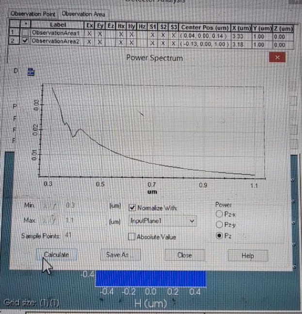
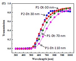
2. If I continue the simulation with the above-attached design (where the rectangular transverse source is normal to the length of the nanowire), I am getting the wrong transmission spectra. An image of the obtained transmission spectra is uploaded. Please check the image file and tell me how will I get the right transmission spectra (I have also uploaded the correct spectra from a reference)
I have a query about the setting up of FWHM.
you have mentioned that width must be larger than the source wavelength.
As we have used 532 nm laser for our experiment, what should be the value of FWHM and time delay?
one more question..As i am interested for calculation of transmittance spectra and reflection spectra, which parameters i should care for?
As you mentioned the design described in No. 1 is correct for my study, i am also curious to know about the design provided in no.2. Is it wrong?
Thank you for your reply.
I am stating the details of the design. please correct me if i am wrong.
As i am new to OPTIFDTD,i have a little bit knowledge in designing and getting the spectra. I have proceeded to measure the spectra with the *.FDA file provided in the FDTD method (https://staging.optiwave.com/forums/topic/silicon-nanowire-fdtd/) and succeded in getting the accurate results for the silicon nanowire with incident light parallel to the nanowire length.
Then i proceeded for the nanowire with incident light normal to the nanowire length where i faced some issues. I came up with two ideas in designing the system.
1: I placed the silicon nanowire parallel to x-axis and the vertical input plane is placed in the positive direction. The detectors (observation areas for transmission spectrum and reflection spectrum ).( I have attached the deisgner file(*FDA) in the previous question)
2: I placed the silicon nanowire along the z-axis with vertical input plane in the positive direction with tilt angle 90 degree.
Are they correct designs for my study?
Also, One more question i want to ask ” How do i know the time delay and FWHM for a particular source wavelength ?”