
Base
| Full Name | park sun geun |
| Organization | postech |
| Job Title | graduate student |
| Country |
Forum Replies Created
Thank you, Scott.
I have another problem.
I make reflectance measurement file and want to see reflectance of angle source. I set 0 degree and 30 degree. but 30 degree source make reflectance more than 1. I know this is a divergence. what is wrong my simulation?
Sungeun
Could you make it? I don’t know how can i do that….
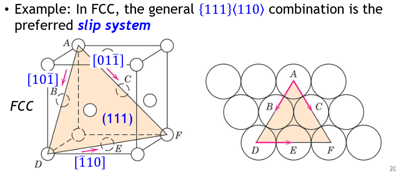
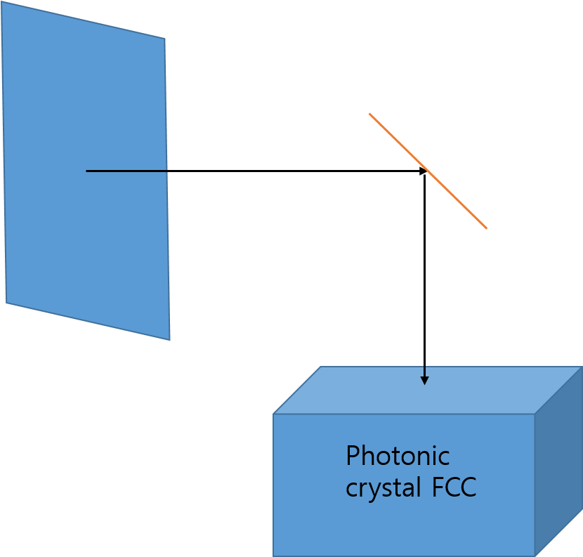
I want to shoot light on the FCC ‘(111)’ side. But optiFDTD PBG Crystal structure can control azimuth angle. FCC 111 structure is similar to Hexagonal Close Packed lattice. source direction is z direction(tilt angle can control y direction). I think this is not enough. If possible, make the incidence ㅣlight perpendicular to the FCC 111 surface. The rotation limitaion seems to let the structure limit the angle of incidence. So, i want to make mirror.
Thank you, Scott
Attachments:
I have more question.
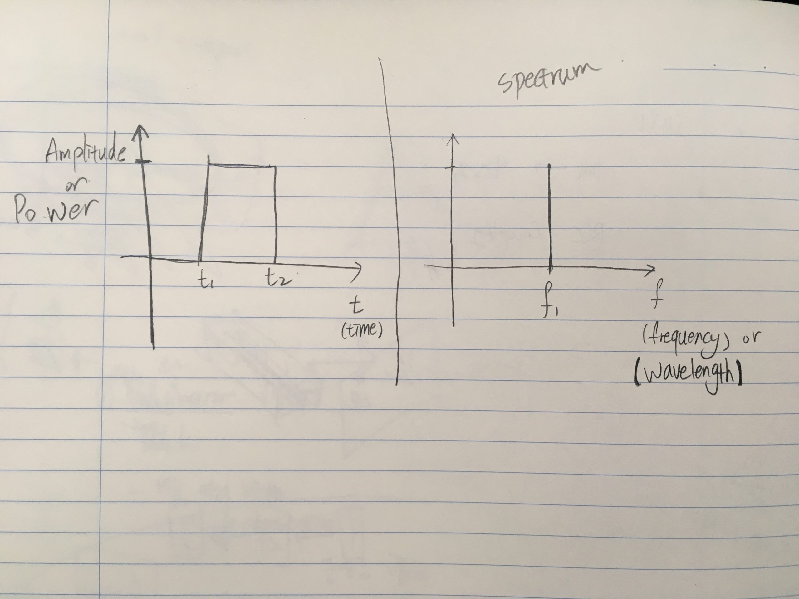
How can I make to particular pulse?
I attach picture.
and Does observation area show the sum of all past light energy or average ?
How can I control the time of observation area?
I don’t know exact mechanism and control method of observation area.
I want to know.
The quality of the question is too low due to lack of knowledge.
please help me
Attachments:
Thank you for answer.
I attach file what i have done.
I try something. I set source that is like RGB white LED spectrum.
I want to see the reflectance, but the amount of reflectance has changed with time.
I guess observation area estimate average of light. is it right?
When i see sample file, that use power spectrum to estimate reflectance.
And i want to know power spectrum y axis. is it power(W)? And then what is mean normalization in power spectrum. I think it is a bit different from what I think.
In conclusion, I would like to see a change in reflectance per wavelength depending on the source I made while changing the photonic crystal.
And I choose sine-modulated gaussian pulse, but In simulation summary, Input type is Gaussian Modulated Continuous Wave. I want you to send me the exact amount.
If there is a sentence that you do not understand, please let me know.