Optiwave software can be used in different industries and applications, including Fiber Optic Communication, Sensing, Pharma/Bio, Military & Satcom, Test & Measurement, Fundamental Research, Solar Panels, Components / Devices, etc..
OptiSystem is a comprehensive software design suite that enables users to plan, test, and simulate optical links in the transmission layer of modern optical networks.
OptiSPICE is the first circuit design software for analysis of integrated circuits including interactions of optical and electronic components. It allows for the design and simulation of opto-electronic circuits at the transistor level, from laser drivers to transimpedance amplifiers, optical interconnects and electronic equalizers.
OptiFDTD is a powerful, highly integrated, and user friendly CAD environment that enables the design and simulation of advanced passive and non-linear photonic components.
OptiBPM is a comprehensive CAD environment used for the design of complex optical waveguides. Perform guiding, coupling, switching, splitting, multiplexing, and demultiplexing of optical signals in photonic devices.
OptiFiber The optimal design of a given optical communication system depends directly on the choice of fiber parameters. OptiFiber uses numerical mode solvers and other models specialized to fibers for calculating dispersion, losses, birefringence, and PMD.
Emerging as a de facto standard over the last decade, OptiGrating has delivered powerful and user friendly design software for modeling integrated and fiber optic devices that incorporate optical gratings.
OptiConverge is a collaborative integration framework that seamlessly combines two or more Optiwave products (e.g., OptiSystem, OptiSPICE, OptiFDTD, etc.) and other third party products into unified solutions. Designed to streamline complex workflows, it empowers users to achieve their goals faster by harnessing the collective power of our trusted Optiwave tools.
Hi thank you for the reply, I do not think there is a physical meaning of a negatig amplitude but the fit is good enough and in the Lorentz-Drude model form (and the fit does not converge with only positive amplitudes).
I still have a question regarding how to fit the permittivity. The convention used by the software is: a loss correspond to a negative imaginary part. For the example shown on the attached picture on the post from November 18, 2015 at 11:38 am, it means the imaginary part should be set as negative before fitting ?
One last question, I tried to set a new material (with Sellmeier model) with the oscillator parameters I found (even if the fit is not perfect) but it seems that negative amplitudes are not supported. How to overcome that ?
I tried Lorentz-Drude, same issue.
I am using the MatLab code that you provided me.
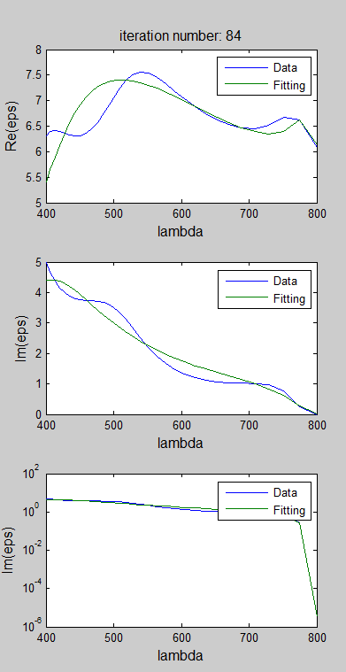
However fitting my data with ‘Lorentz Drude’ model appears not to be very accurate (see attached the best result I can get using 6 oscillators).
Would it be possible to import the data directly from XML format ?
Damian, thank you for the reply, it helped me a lot ! You are right for the structure and I finaly did not use the PBG structure at all. Can I ask for 3 more questions about structure design ?
I want to simulate surface plasmons in a thin Ag layer (~40 nm thick) deposited on glass. The layer is perforated with a 2D array of circular air holes (close packed lattice, with lattice parameter 0.562nm). Light is propagating through the glass, the perforated Ag layer and then the air medium.
– I chose the simulation domain to be glass (n=1.5).
– I adjusted the simulation domain dimensions in order that it matches with the unit cell of my structure and used periodic boundaries conditions.
– I created a linear waveguide of silver (40 nm thick).
– I created cylinders made of air, their centers are separated by the pitch (562 nm).
– I created a linear waveguide of air.
I put in attached the final design, could you take a look at it ? I have two issues about it.
First, I wonder what would be the difference between a 3D block of Ag and the linear waveguide profile used ?
Then, some cylinders are not entirely in the simulation domain in order to define the unit cell, is that a problem ?
Finaly, I wish to study the structure not only at normal incidence but with an angle, how is that possible ? By tilting the imput plane or the structure (then I will have issues with the periodic conditions to define the 2D array…)
It would really help me if you had some piece of advice,
Thank you a lot !
Nathalie