
Base
| Full Name | Natalia Rebrova |
| Organization | Tyndall |
| Job Title | Dr. |
| Country |
Forum Replies Created
No, sorry, I haven’t tried that one
Hi Harkiranjeet,
It is still larger but marginally, like 1.00005 so I guess this is just computational errors piling up and this can be ignored.
What helped me to solve the issue was 2 things. First I enlarged a bit the free space between the grating and input line. My dimensions are 7 microns device and 20 microns free space. Second, I increased the number of time steps there was insufficient number of them. I had 10000 and 60000 or 100000 solved the issue.
Hope this helps,
Natalia
I think I found the problem. It was insufficient timesteps number for this size.
I have ricwaa calculations. I’m comparing against them. See the plot attached
Attachments:
Thanks again for help.
I tried to run your file. And it still shows normalized power more than one.
I also played with distances and it seems that the spectrum is different depending on where I put the input field plane. Why is that?
Dear Damian,
I can’t open the file cause my version is 32 bit. Could you please save the file in other format, our describe what to change.
In particular I can’t find where do I set these
Also the DFT spectrum you specified wasn’t reflected by the simulation parameters. I think it was set to something like 0.4 to 0.8 um, so I changed it to 7.5 um to 12.5 um.
I don’t see any wavelength changes in simulation parameters dialog.
Thank you very much for your help.
Hi, Damian,
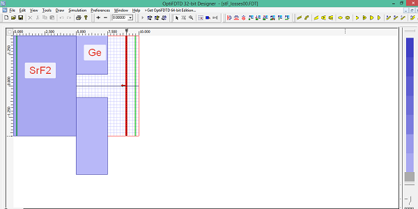
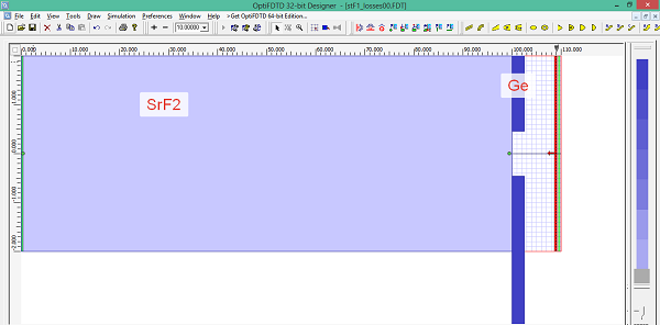
I attached my file.
Basically, what I need to calculate is reflection coefficients over 7.5 – 12.5 mu.
Thank you for your help.
Best regards,
Natalia
Attachments:
Dear Damian,
Thank you for the answer.
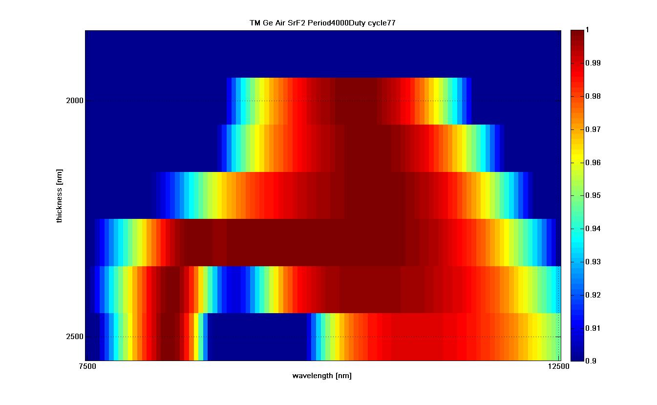
About the substrate what I meant is the situation on the attached pictures. I am getting different reflection spectra depending on the thickness of SrF2 layer. If I model the same situation say in ricwaa it wouldn’t be the case.
I thought may be it’s possible to modify initial conditions in a way that the lower side of the substrate is considered infinite?
Best regards,
Natalia Rebrova
Attachments:
Hello, David.
Thank you very much for your answer it is very helpful.
About normalization on observation line. What got me confused is that sometimes I get values larger than one after normalization.
Best regards,
Natalia