
Base
| Full Name | Malik Javaid |
| Organization | High School |
| Job Title | Student |
| Country |
Forum Replies Created
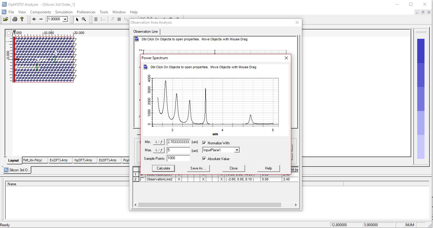
I ran the simulation at the lower mesh size, as you said, but the results I received were similar to the results shown above.
I also read that increasing the amount of PMLs in the simulation could reduce error, however, that also did not yield accurate results for me. Can you help me find other ways to decrease the error in the graph and get accurate results?
Attachments:
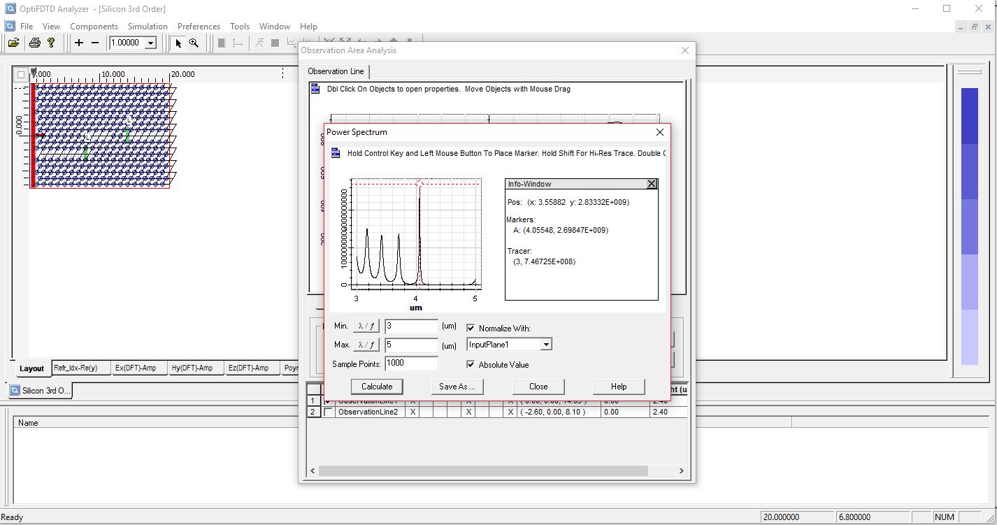
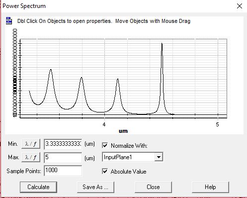
I ran the simulation again with a source of 4.5um and I received the graph shown where the peak is 4.055um. I then ran the simulation once again with a source of 4.055um and I received a transmission graph different than the one I had gotten before. Why is this the case?
I apologize, I attached the wrong file. Here is the correct one.
Attachments:
https://www.photonics.com/a63226/All-Optical_Logic_Gates_Show_Promise_for_Optical
This article is the reference I am using. I am trying to replicate what they have built, except instead of using one input waveguide, I am planning on using two with different intensities so that the waveguide with the greater intensity light is able to control the other waveguide’s light using nonlinear properties. This article is also supported by the book you had referred to me, Photonic Crystals: Modeling the Flow of Light, on pages 214-218 and by the screenshot I have attached to this post which I had posted before. This screenshot is on page 197 of the book.
Here is the link to the book in case you need it:
http://ab-initio.mit.edu/book/photonic-crystals-book.pdf
Also, the transmission spectrum I have attached above is in fact for the structure with the resonator and waveguides.
Attachments:
Oh I thought I had attached them, I guess they didn’t attach.
I found the transmission spectrum attached, but when I run the FDTD simulation with the peak power in the graph, 4.508 um, the results don’t match what I found in the graph.
What do you mean by centered at the waveguide with the correct width? How do you find the correct center and width?
Thank you so much for recommending the book. I consulted it, and I realized what I was looking for. I was not looking for the PWE simulation, but instead I was looking for a transmission spectrum, where it shows at which frequency the mode will propogate in the cavity. Is it possible to simulate this in the software?
Attachments:
I understand what you are trying to say, and I will use the larger band gap for my design. Is my assumption correct that the defect bands within the original bandgap are the wavelengths which will resonate in the cavity? Which means the wavelengths not in the defect bands but still in the bandgap will not resonate in the cavity but will propogate through the linear waveguide?
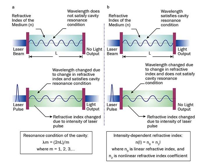
Also, in one of my references, it talks of a resonance condition of a cavity, which is the wavelength which will resonate in the cavity and not escape the cavity. What I am trying to do is find this resonance condition so that if I introduce a linear waveguide right after the cavity, the light will not propogate into the waveguide due to the resonance condition. I ran the PWE simulation because I assumed the defect bands would correspond to the resonance condition, but after reading your comments I am not so sure anymore. Is it possible to simulate this condition, and if so, how?
I attached an image of what I mean when I say resonance condition.
Attachments:
I don’t see an attached image. Could you please reattach it?
Oh I apologize let me reattach them.
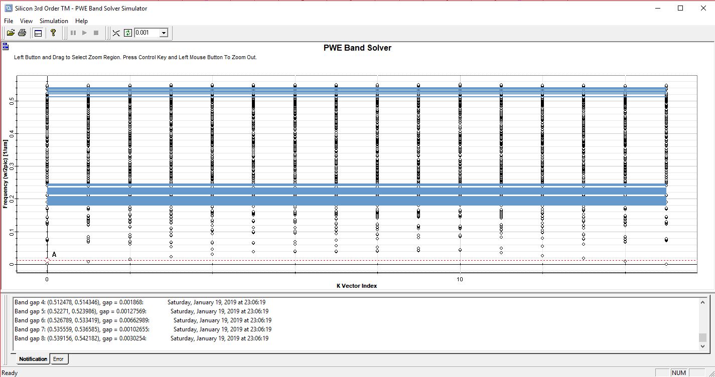
I ran the PWE simulation and I received the solutions within the bandgap. However, when I ran the 2D FDTD simulation using a solution as a wavelength parameter, the wave was not propogating through the cavity at all. Do I have the wrong solution, or is there something else at play?
I’ve attached my design file, along with a screenshot of the PWE simulation output. I chose 0.535 (w/2pic), which is in between band gaps 6 and 7, and converted it to um as my parameter.
Is there any way to find the bandgap taking into consideration the power other than the PWEM calculation?