Optiwave software can be used in different industries and applications, including Fiber Optic Communication, Sensing, Pharma/Bio, Military & Satcom, Test & Measurement, Fundamental Research, Solar Panels, Components / Devices, etc..
OptiSystem is a comprehensive software design suite that enables users to plan, test, and simulate optical links in the transmission layer of modern optical networks.
OptiSPICE is the first circuit design software for analysis of integrated circuits including interactions of optical and electronic components. It allows for the design and simulation of opto-electronic circuits at the transistor level, from laser drivers to transimpedance amplifiers, optical interconnects and electronic equalizers.
OptiFDTD is a powerful, highly integrated, and user friendly CAD environment that enables the design and simulation of advanced passive and non-linear photonic components.
OptiBPM is a comprehensive CAD environment used for the design of complex optical waveguides. Perform guiding, coupling, switching, splitting, multiplexing, and demultiplexing of optical signals in photonic devices.
The optimal design of a given optical communication system depends directly on the choice of fiber parameters. OptiFiber uses numerical mode solvers and other models specialized to fibers for calculating dispersion, losses, birefringence, and PMD.
Emerging as a de facto standard over the last decade, OptiGrating has delivered powerful and user friendly design software for modeling integrated and fiber optic devices that incorporate optical gratings.
OptiConverge is a collaborative integration framework that seamlessly combines two or more Optiwave products (e.g., OptiSystem, OptiSPICE, OptiFDTD, etc.) and other third party products into unified solutions. Designed to streamline complex workflows, it empowers users to achieve their goals faster by harnessing the collective power of our trusted Optiwave tools.
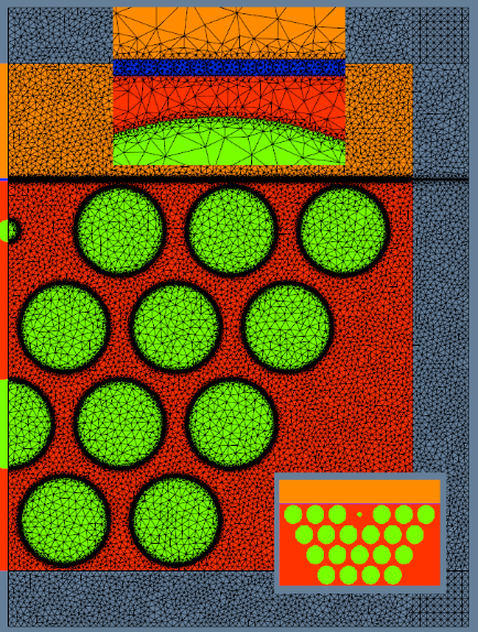
Photonic crystal fibers (PCF) are attractive for chemical, biomedical, and environmental sensing applications. The freedom in designing the microstructure geometry provides a unique platform for realizing the desired modal dispersion, birefringence, confinement, and multiplicity characteristics. Of significant importance to these features, chemical, biological and inorganic materials can be introduced to the PCF by selective hole infiltration or deposition techniques. Novel PCF sensor designs often encompass structural and electromagnetic field features spanning multiple orders of magnitude in variation, e.g., sub-wavelength metal films and tightly confined surface plasmonic modes in a PCF with wavelength-scale mode and air-hole radii having cladding dimensions of 100 times of the wavelength. These properties require a mode solver that can both efficiently and accurately approximate the geometry and the electromagnetic fields over the entire simulation domain.
Simulation domain with the FEM mesh superimposed. (Lower inset) schematic of the PCF. (Top inset) a zoomed view of the mesh at the metal-dielectric interfaces and a hole boundary.