In this tutorial, we demonstrate the simulation of a VCSEL Array circuit that contains an array of Vertical Cavity Surface Emitting Lasers (VCSEL) which exhibits temperature dependent effects.
Sample: Vcsel Array.osch
Figure 1: Schematics of VCSEL Array
This circuit contains an array of eight VCSELs. The top level schematics contain eight subcircuit block representing each VCSEL channel. VCSEL in each channel is driven by the pulse voltage source Vpulse1 and the DC power for each channel is provided by DC voltage source Vpower. The Vpulse generates a pulse with initial value of 1.25 V and a peak value of 3.75 V. After the one pulse it remains at the initial value of 1.25 V.
Thermal conductance between adjacent channels are set by the thermal resistors RTH12, RTH23, RTH34, …, and RTH78. The thermal resistances of these resistors are given by the user defined global parameter CROSSRTH which is defined to be 500 K/W.
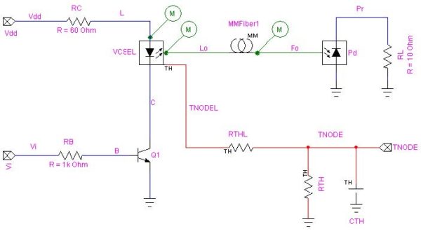
Figure 2 shows the internals of the subcircuit block for a single VCSEL channel. The subcircuit block can be opened by pressing CTRL+SHIFT+I keys together.
Figure 2: Subcircuit block of a VCSEL channel
The device symbol for the VCSEL is from Laser – Thermal device from OptoElectronic library. The VCSEL operates at the wavelength of 863 nm (347.384 THz). The model parameters for the VCSEL are obtained based on the parameters provided by [1].
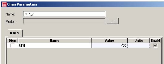
The temperature rise of the VCSEL from global circuit temperature (25°C) is set by the temperature value at the thermal node TNODEL. The thermal resistance between TNODEL and TNODE is given by RTHL which has a thermal resistance of 50 K/W. TNODE has a thermal resistance given by subcircuit parameter RTH and thermal capacitance of 0.001 J/K with the global circuit temperature (thermal ground represents the global circuit temperature). The value of the subcircuit parameter RTH is set at the top level circuit and it is varying for each block. As thermal resistance value gets higher, the ability to dissipate heat will be lower. As a result, channel blocks with higher RTH values will have high laser temperatures. To view the RTH value for each block, right click on a subcircuit block and select Parameters. Figure 3 shows the RTH value for the channel 2.
Figure 3: Thermal resistance parameter RTH for channel 2
The VCSEL is connected to the photodiode Pd via a multi-mode fiber, MMFiber1. When a pulse voltage is applied to Vi at the base of the bipolar junction transistor Q1, the laser current will start to pulsate and as a result, the VCSEL will have a corresponding response in the output power. The Q1 also has temperature dependence and TNODE is given as its external temperature node. Due to the thermal network and the difference in RTH value for each VCSEL channel, a variance in VCSEL current and output power between each channel can be expected.
Probes are placed on the subcircuit block for VCSEL current, VCSEL optical output, and optical output after fiber. This will produce three probes for each block and as a result simulation has to produce output for 24 probes.
Analysis:
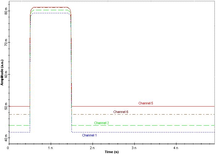
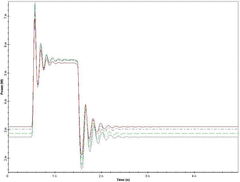
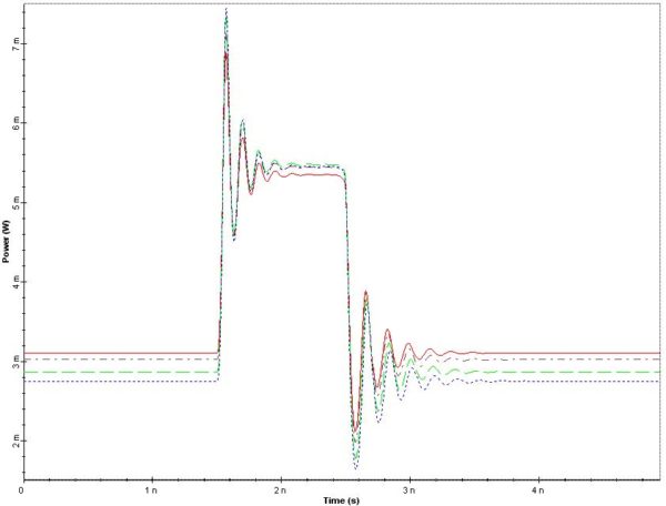
Transient analysis for this circuit is performed for 5 ns time period.Figure 4 shows the VCSEL current for channels 1, 2, 5, and 6. Figure 5 and Figure 6 show the optical output power for those channels at the VCSEL and after the MMFiber1.
As you can see from the graphs, due to the temperature effects modeled using the thermal network, current and the output power vary between each channels.
Figure 4: VCSEL currents for channel 1, 2, 5, and 6
Figure 5: VCSEL optical output for channel 1, 2, 5, and 6
Figure 6: Optical output after fiber for channel 1, 2, 5, and 6
References:
[1] P. V. Mena, J. J. Morikuni, S. M. Kang, A. V. Harton and K. W. Wyatt, “A Simple Rate-Equation-Based Thermal VCSEL Model”, J. Lightwave Technology, vol. 17, pp. 865-872, May 1999.


