This lesson describes how to create a chip-to-fiber coupler. You will create a model of a simple spot-size transformer based on lateral tapering, as reported in [1].
Highly efficient chip-to-fiber coupling with large alignment tolerances is important for applications of optoelectronic integrated semiconductor devices. Such coupling requires a low-loss change of the light beam spot from about 1μm of the mode to the 8-10μm range for the guided mode in the fiber.
A two-layer spot-size transformer is shown in Figure 1. The device consists of a strongly guiding two-layer input waveguide and a weakly guiding output waveguide with a two layer laterally tapered section between them. We will be considering dimensions and materials as given in [1] (Table 7). Details of the production process can also be found in the reference [1].
Figure 1: Two-layer spot-size transformer
| Material | Parameter |
| nCladding (InP) | 3.1662 |
| nSubstrate (InP) | 3.1662 |
| nTopLayer (InGaAsP_top) | 3.3832 |
| nBottomLayer (InGaAsP_bottom) | 3.2416 |
| Ltaper | 560μm |
| WInputTop | 1.2μm |
| WInputBottom | 2.4μm |
| dCladding | 5μm |
| dBuffer | 0.4μm |
| dSubstrate | 5μm |
| dTopLayer | 0.3μm |
| dBottomLayer | 0.11μm |
| WOutputTop | 0.08μm |
| WOutputBottom | 6.0μm |
Table 7: Materials and parameters
Before you start this lesson
- Familiarize yourself with the procedures in Lesson 1: Getting Started.
- Familiarize yourself with the procedures in Lesson 2: Create a simple MMI coupler.
- Familiarize yourself with the procedures in Lesson 3: Create a single-bend device
The procedures include:
- Defining materials and waveguides for the chip-to-fiber butt coupler
- Defining the layout settings
- Creating a chip-to-fiber butt coupler
- Editing the Input plane
- Setting the simulation parameters
- Running the simulation
Defining materials and waveguides for the chip-to-fiber butt coupler
To define the materials and channels for the chip-to-fiber butt coupler, perform the following procedure.
| Step | Action |
| 1 | Create the following dielectric material: Name: InGaAs_bottom 2D Isotropic Refractive Index (Re): 3.2416 3D Isotropic Refractive Index (Re): 3.2416 |
| 2 | Create a second dielectric material: Name: InP 2D Isotropic Refractive Index (Re): 3.1662 3D Isotropic Refractive Index (Re): 3.1662 |
| 3 | Create a third dielectric material: Name: InGaAs_top 2D Isotropic Refractive Index (Re): 3.3832 3D Isotropic Refractive Index (Re): 3.3832 |
| 4 | Create the following channel profiles: Profile Name: InputWgChannel Layer 1: Layer Name: BottomLayer Width: 2.4 Thickness: 0.11 Offset: 0.0 3D Profile definition material: InGaAs_bottom Layer 2: Layer Name: TopLayer Width: 1.2 Thickness: 0.3 Offset: 0.0 3D Profile definition material: InGaAs_top Profile Name: TopInGaAsChannel Layer Name: top Width: 1.0 Thickness: 0.3 Offset: 0.0 3D Profile definition material: InGaAs_top Profile Name: BottomInGaAsChannel Note: The 2D parameters are not going to be used. The structure can be clearly simulated only in 3D. |
Defining the layout settings
To define the layout settings, perform the following procedure.
| Step | Action |
| 1 | Type the following settings. a.Wafer Dimensions: Length: 700 Width: 20 Cladding: Material: InP Thickness: 5.4 Substrate: Material: InP Thickness: 5.0 |
| 2 | To apply the settings to the layout, click OK. Note: There is no need to make the simulation space too wide as there should not be a large scattering within the domain. |
Creating a chip-to-fiber butt coupler
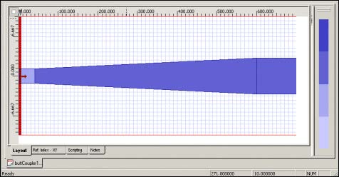
The input waveguide will be defined as a 2-layer single channel and the output waveguide as a simple one layer channel. To model the tapered part of the coupler, we will decompose it into 2 separate single layer channels positioned on top of each other. Each one of the channels will be a linear taper waveguide with tapering in opposite directions.
To create the chip-to-fiber butt coupler, perform the following procedure.
| Step | Action |
| 1 | Draw and edit the straight input waveguide. a.Start offset: Horizontal: 0 Vertical: 0 b.End Offset: Horizontal: 40 Vertical: 0 c.Width: 2.4 d.Depth: 0.4 e.Label: Linear Input Waveguide f.Profile: InputWgChannel |
| 2 | Draw and edit the bottom tapered waveguide. a.Start Offset: Horizontal: 40 Vertical: 0 b.End Offset: Horizontal: 600 Vertical: 0 c.Start Width: 2.4 d.End Width: 6.0 e.Depth: 0.4 f.Label: Taper Linear Bottom g.Profile: BottomInGaAsChannel |
| 3 | Draw and edit the straight output waveguide. a.Start Offset: Horizontal: 600 Vertical: 0 b.End Offset: Horizontal: 700 Vertical: 0 Note: Notice the Depth Parameter values are set to 0.4. This will place the bottom of the waveguides 0.4 micrometers above the substrate, leaving a space for the buffer layer. As the buffer is of the same material as the cladding and substrate, there is no need for further concern. |
Figure 2: Layout design
| 4 | Draw and edit the top tapered waveguide. Note: To ensure that the top waveguide is on top of the bottom one, make sure the depth of the top waveguide is set to (buffer + bottom layer thickness) 0.4 + 0.11 = 0.51. a.Start Offset: Horizontal: 40 Vertical: 0 b.End Offset: Horizontal: 600 Vertical: 0 |
| 5 | Insert the input plane. |
Editing the Input plane
To edit the input plane values, perform the following procedure.
| Step | Action |
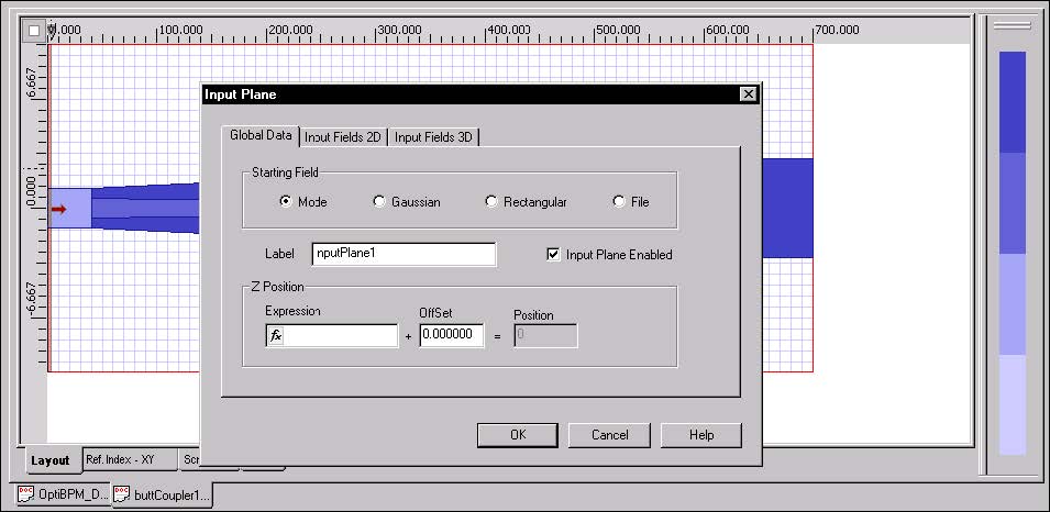
| 1 | Double-click the input plane. The Input Plane dialog box appears (see Figure 3). |
| 2 | Type the following values: a.Starting Field: Mode b.Z Position: 0 |
| 3 | Click the Input Fields 3D tab. |
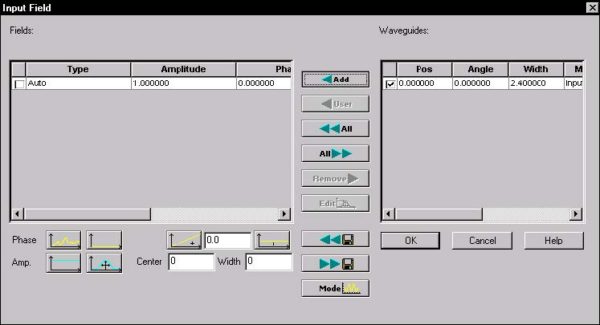
| 4 | Click Edit. The Input Field dialog box appears (see Figure 4). |
| 5 | In the window under Waveguides, select the check box (see Figure 4). |
| 6 | Click Add. The item under Waveguides moves into the window under Fields. |
| 7 | To return to the Input Plane dialog box, click OK. |
| 8 | To return to the layout window, click OK. |
Figure 3: Input Plane dialog box
Figure 4: Input Field dialog box
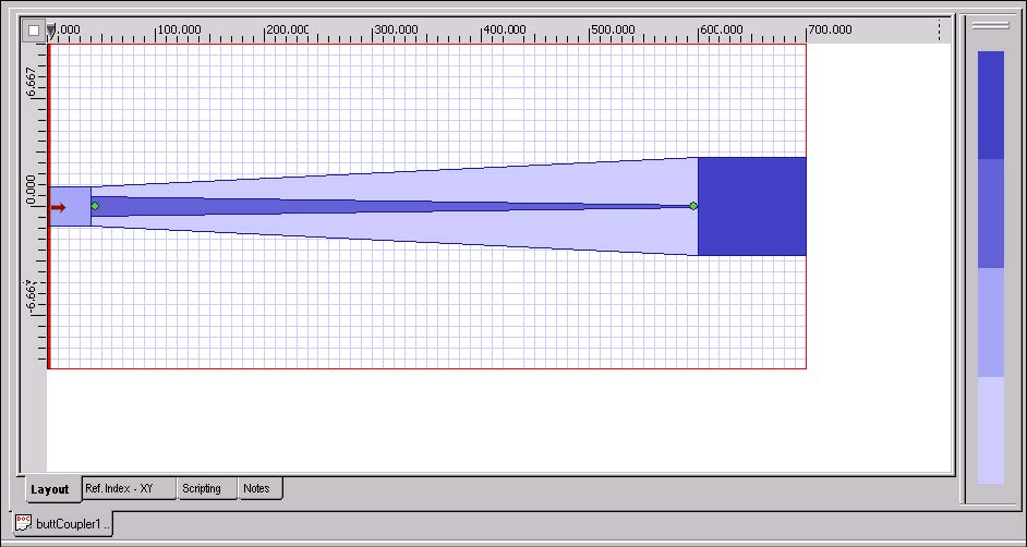
The resulting layout should be similar to the one found in Figure 5.
Figure 5: Layout design with top waveguide
Setting the simulation parameters
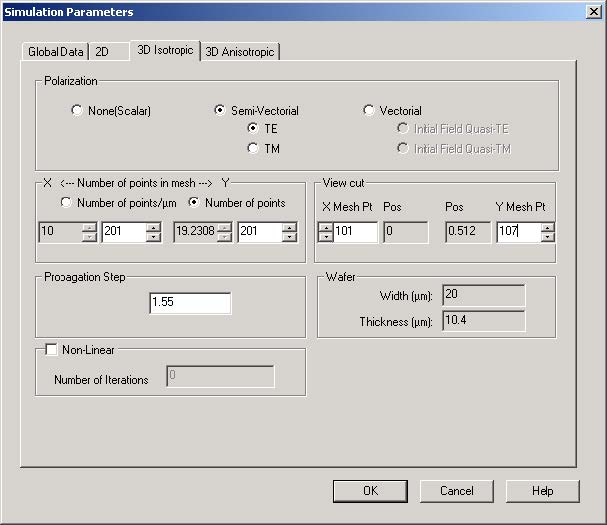
When setting the simulation parameters, adjust the number of mesh points so that the resolution of the results is satisfactory (in this case, 201×201).You may also want to adjust the View Cut coordinates so that you can observe cuts through the areas of interest during the simulation. In this example, the viewing planes cross both the waveguide in the vertical direction (x~0.0) and the bottom waveguide in the lateral direction (y~0.5).
To set the simulation parameters, perform the following procedure.
| Step | Action |
| 1 | From the Simulation menu, select Simulation Parameters. The Simulation Parameters dialog box appears. |
| 2 | Click the Global Data tab and type the following settings: a.Reference Index: Modal b.Wavelength: 1.550000 c.Number of displays: 100 |
| 3 | Click the 3D Isotropic tab and type the following settings: a.Polarization: Semi-Vectorial, TE b.Number of points: 201 x 201 c.View cut: i.X Mesh Pt: 101 (x-position ~ 0) ii.Y Mesh Pt: 107 (y-position ~ 0) d.Propagation Step: 1.55 |
Running the simulation
To run the simulation, perform the following procedure:
| Step | Action |
| 1 | From the Simulation menu, select Calculate 3D Isotropic Calculation. The Simulation Parameters dialog box appears. |
| 2 | Click the 3D tab and check the settings (see Figure 6). |
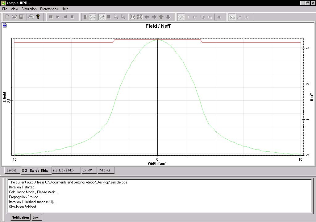
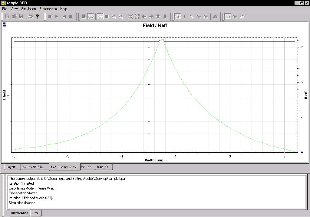
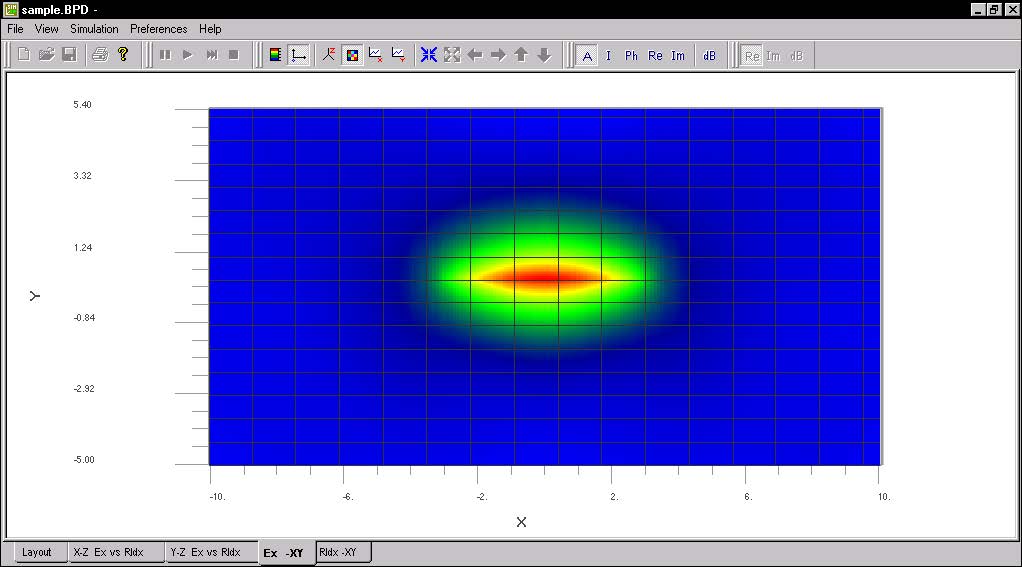
| 3 | Start the simulation. The results appear in the layout. See Figure 7, Figure 8, and Figure 9 for result examples. |
Figure 6: Simulation Parameters dialog box
Figure 7: X-Z Ex vs RIdx results
Figure 8: Y-Z Ex vs RIdx results
Figure 9: Ex XY results — 2D
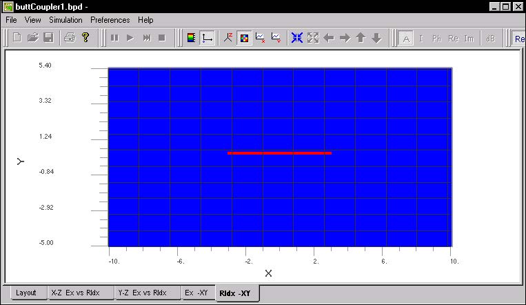
Figure 10 RIdx-XY results — 2D
References
[1] R. Zengerle, O. Leminger, W. Weiershausen, K. Faltin, and B. Huebner: Laterally tapered InP- InGaAsP waveguides for low-loss chip-to-fiber butt coupling: A comparison of different configurations, IEEE Phot. Techn. Lett. 7, (May 1995): 532-534.


