Applications
- Backbone aggregation to replace N*10 G LAG.
- Data center network aggregation and enterprise computing.
- Convergence of Transport and Ethernet at 100 G-Ethernet transport.
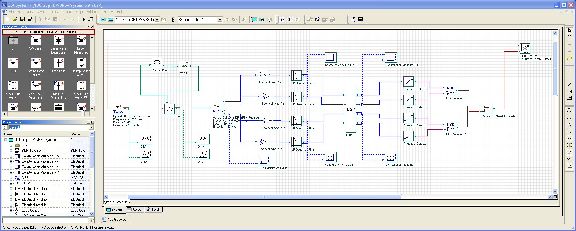
100 Gbps DP-QPSK Layout
Benefits
- Significantly reduces product development costs and boosts productivity through a comprehensive design environment to help plan, test, and simulate optical links in the transmission layer of modern optical networks.
- Enables users to analyze different algorithms for the electronic equalization (ex. Gram-Schmidt orthogonalization procedure (GSOP), Ellipse correction method (EC), transversal digital filter)
- Interfaces with popular design tools.

- New BER Test Set enables the simulation of millions of bits for direct error counting.
- FEC
- Multi-parameter scanning enables system designers to study trade-offs with respect to parameters of interest and to choose an optimal design for deployments.
- Explores different modulation formats for 100G: DQPSK, coherent DP-QPSK, coherent OFDM, and coherent M-QAM.
Simulation Description
The 100 Gbps DP-QPSK system can be divided into five main parts: DP-QPSK Transmitter, Transmission Link, Coherent Receiver, Digital Signal Processing, and Detection & Decoding (which is followed by direct-error-counting). The signal is generated by an optical DP-QPSK Transmitter, and is then propagated through the fiber loop where dispersion and polarization effects occur. It then passes through the Coherent Receiver and into the DSP for distortion compensation. The fiber dispersion is compensated using a simple transversal digital filter, and the adaptive polarization demultiplexing is realized by applying the constant-modulus algorithm (CMA). A modified Viterbi-and-Viterbi phase estimation algorithm (working jointly on both polarizations) is then used to compensate for phase and frequency mismatch between the transmitter and local oscillator (LO). After the digital signal processing is complete, the signal is sent to the detector and decoder, and then to the BER Test Set for direct-error-counting.
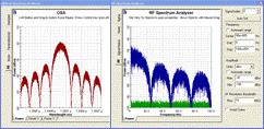
Below is an image of the optical spectrum of the 100 Gbps DP-QPSK signal after the transmitter, as well as the RF spectrum obtained after the Coherent DP-QPSK Receiver.
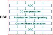
The inner structure of the DSP modules is shown below:
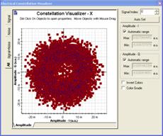
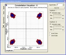
The electrical constellation diagrams (for polarization X) before and after the DSP are as follows:
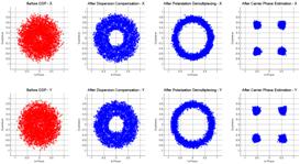
The algorithms used for digital signal processing are implemented through a Matlab component. By setting the Matlab component to debug mode, the generated electrical constellation diagrams after each step (CD compensation, Polarization Demultiplexing, and Carrier Phase Estimation) are shown here:


